Overview
Image
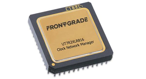
UT7R2XLR816 Clock Network Manager

The UT7R2XLR816 is a low voltage, low power, clock network manager.

The device features 16-outputs in 8 banks of 2. Independent power supplies for each bank give the user great flexibility in multi-voltage systems. Well-suited for high altitude avionics, networking, telecommunications and mass storage, independent output bank division and phase skewing enable the system designer to optimize output phase and frequency relationships throughout a clock network.

Image left, text right (default)
Overview
Key Tech Specs
  • Features:
  • 8 Output clock Banks with Flexible I/O Signaling
  • +3.3V Core Power Supply
  • 750KHz to 200MHz
  • Independent Power Supply for each Clock Bank
  • Input Clock Multiplication of any Integer from 1 – 32
  • PLL Operation
  • Input Reference Clock Signaling and Control
  • Dedicated Feedback Input/Output Module
  • Output Clock Bank Signaling and Control
  • Guaranteed Reference Input to Output Edge
  • Low Inherent Output Bank Skew
  • Power Dissipation can be Reduced by Power Down Unused Output Banks
  • Applications:
  • High Altitude Avionics
  • X-ray Cargo Scanners
  • Test and Measurement
  • Networking, Telecommunications and Mass Storage 
  • Operational Environment:
  • Temperature Range: -55°C to +125°C
  • Total Ionizing Dose: <100 krad (Si)
  • SEL Immune: ≤109 MeV-cm2/mg
  • SEU Immune: ≤109 MeV-cm2/mg
  • Physical:
  • 168-Pin CLGA, CBGA, CCGA, 17mm x 17mm, 1.27mm Pitch
  • Power:
  • 1mW/MHz
  • Flight Grade:
  • QML-Q, QML-Q+
  • Export Control Classification Number (ECCN):
  • 9A515.e.1
  • SMD Number:
  • 5962-08243

ADDITIONAL SPECIFICATIONS

Defense Logistics Agency

Key Tech Specs
Downloads

Application Notes

CCGA Application Notes


Datasheet

Datasheet-UT7R2XLR816.pdf


IBIS Model

ut7r2xlr816.ibs

Downloads
Support

Do you need help with an existing product?

Our customer and technical support teams are happy to assist.

Support